iPhone 17 is coming soon: The role of machine tools in the semiconductor manufacturing steps behind the A19 Pro chip.
As the release of the iPhone 17 approaches, tech enthusiasts are eagerly anticipating the powerful performance boost brought by the new A19 Pro chip. According to the latest news, the performance of the A19 Pro chip will see a significant upgrade, with Geekbench 6 scores expected to reach over 4000+ for single-core and over 10000+ for multi-core, marking a notable increase compared to the previous A18 Pro's single-core 3500+/multi-core 9000+ performance. Behind the strong performance of this generation of chips lies the precision processes involved in semiconductor manufacturing, where machine tools also play a crucial role.
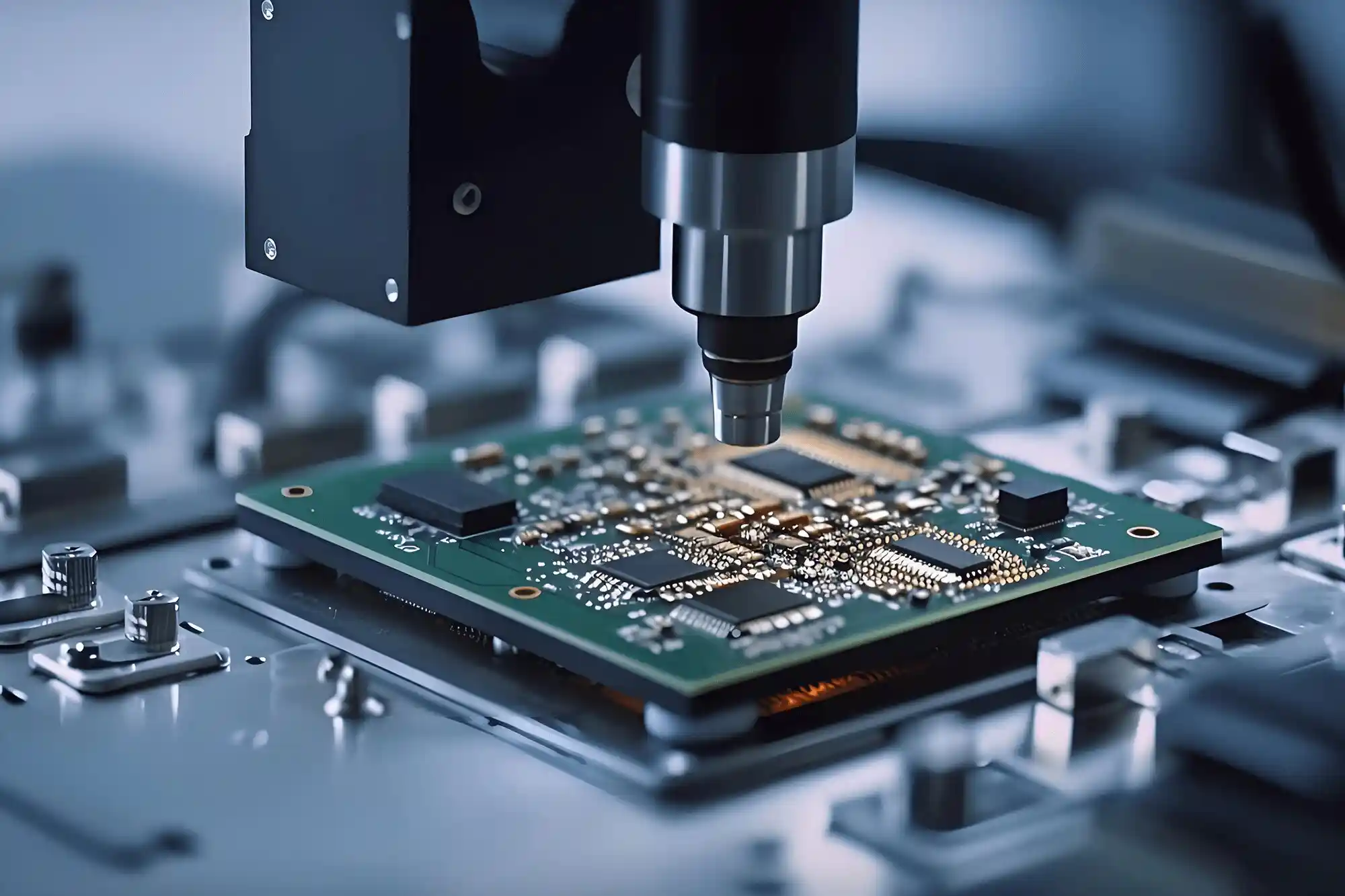
In semiconductor production, especially in the manufacturing of high-end chips like the iPhone 17's A19 Pro chip, several complex steps are involved, including deposition, lithography, etching, and ion implantation. Machine tools ensure the precision and quality of the chip during the early-stage cutting, packaging, and surface processing.
Today, let's discuss which steps in semiconductor manufacturing require machine tools and how they help enhance chip performance.
I、What are Semiconductors and Semiconductor Materials?
Semiconductors are materials with electrical conductivity between that of conductors (such as copper and aluminum) and insulators (such as rubber and plastic). The unique feature of semiconductors is that their electrical conductivity can be precisely controlled by external factors like temperature, light exposure, and doping with other elements. This ability makes them a core material for manufacturing electronic components.
Common semiconductor materials include elemental semiconductors, compound semiconductors, and alloy semiconductors.
Among elemental semiconductors, silicon (Si) is the most widely used, holding a dominant share in the semiconductor market. This is due to silicon's abundance in nature, mature purification processes, and stable performance. Most of the chips we use daily are based on silicon. Germanium (Ge) is also an important elemental semiconductor, which was widely used in early semiconductor devices and still finds application in certain high-frequency devices today.
Compound semiconductors, such as gallium arsenide (GaAs) and indium phosphide (InP), excel in high-frequency, high-speed, and optoelectronic applications, such as in 5G communication, satellite communication, and light-emitting diodes (LEDs).
II、Six Key Steps in Semiconductor Production
Semiconductor manufacturing is a highly precise and complex process, involving several critical steps. Here are the six key steps summarized:
Deposition
In this step, materials are deposited onto the surface of a silicon wafer through technologies like physical vapor deposition (PVD) or chemical vapor deposition (CVD), forming thin films. This is the first step in building the basic structure of a semiconductor chip.Photoresist Coating
This step involves evenly coating the silicon wafer with photoresist (a light-sensitive material) in preparation for the subsequent photolithography process. The uniformity and surface smoothness of the coating are critical to ensuring precise pattern transfer.Lithography
Photolithography is the process of transferring a design pattern onto the silicon wafer. Using ultraviolet light, the pattern is precisely transferred onto the photoresist-coated wafer, laying the foundation for the formation of the chip's circuits.Etching
 Etching uses chemical or physical methods to remove unwanted material, exposing the designed circuit pattern. This step precisely removes material outside the pattern to create space for the electrical connections of the chip.
Ion Implantation
Ion implantation involves accelerating ions and embedding them into the silicon wafer to alter its electrical properties. This process is mainly used to change the conductivity of the material and lays the foundation for the semiconductor devices' functionality.Packaging
Packaging is the process of connecting the completed chip's circuit to the external world. It not only protects the chip from physical and chemical damage but also ensures stable and reliable electrical connections between the chip and other electronic components.III、How do machine tools support the manufacturing of the iPhone 17's A19 Pro chip
The performance improvement of the A19 Pro chip relies on precise control in each manufacturing step. While processes like deposition, photolithography, and ion implantation are critical, the fine-tuning of post-processing and packaging also determines the final chip quality. For example, in the packaging process, CNC machine tools and laser cutting machines are used for micro-machining, precision cutting, and the processing of the chip's housing, ensuring the chip's size, shape, and final performance.
Furthermore, in post-packaging surface processing, polishing machines ensure the silicon wafer's surface is smooth, removing any tiny defects that could affect the chip's performance, greatly improving yield rates.
By optimizing the production process with precision machine tools, manufacturers can minimize micron-level errors, further enhancing the chip's performance. Behind every A19 Pro chip, these high-precision machines are silently supporting the process.
IV、Special Machine Tools in Semiconductor Material Processing
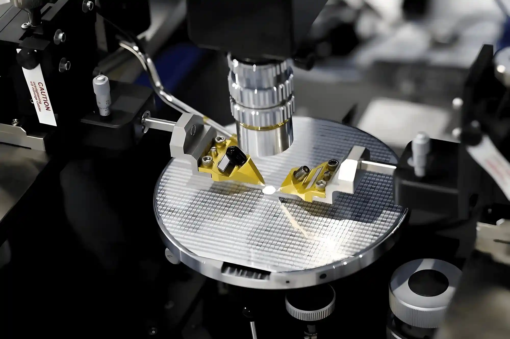
In addition to playing a role in chip packaging, special machine tools are also crucial in the early-stage processing of semiconductor materials. Silicon, as the primary material for semiconductor chips, relies heavily on specialized machine tools during the processing of raw silicon ingots.
Silicon ingots must undergo cutting, grinding, and polishing to become usable silicon wafers. Multi-wire cutting machines are key equipment for slicing silicon ingots. By using high-speed metal wires, the multi-wire cutting machine slices the silicon ingot into uniformly thick wafers. Compared to traditional cutting methods, multi-wire cutting machines offer advantages like higher cutting efficiency and less surface damage, making them ideal for large-size silicon wafer production. This greatly helps improve material utilization and processing efficiency in the production of A19 Pro chips.
V、Conclusion
While processes like deposition and photolithography are less related to traditional machine tools, machine tools play a crucial role in the later stages, such as cutting, packaging, and surface processing. These steps ensure the high quality and consistency of the final product.
As a professional machine tool solution manufacturer, Minnuo understands the precision machine tool needs in semiconductor manufacturing. Whether it's CNC machine tools for packaging or multi-wire cutting machines for material processing, if you have any machine tool needs in semiconductor manufacturing, feel free to contact us. Let's work together to support the continuous breakthroughs in semiconductor technology.

 Email
Email sales1: +86 13295238763